SAKIGAKE Semiconductor Co., Ltd. has firmly established itself as a leader in plasma technology, specializing in both atmospheric pressure and vacuum plasma applications. Their expertise spans surface modification, etching, thin-film deposition, cleaning, sterilization, adhesion enhancement, and water- and oil-repellent treatments. With continuous innovation, SAKIGAKE is driving the evolution of plasma processing in the semiconductor industry and beyond. This article explores their recent advancements, technological breakthroughs, and industry applications.
Cutting-Edge Plasma Power Supply: PKM-VP20
In June 2024, SAKIGAKE Semiconductor introduced the “PKM-VP20” AC High-Voltage Power Supply, designed for compact vacuum plasma equipment. This power supply sets new benchmarks in efficiency, compactness, and performance. By leveraging unique circuit technology, the PKM-VP20 achieves a significant reduction in size and weight, simplifying installation and handling. Operating at a high frequency of approximately 80–100 kHz, it ensures stable plasma treatment across a wide range of materials. Additionally, its energy-efficient design minimizes heat generation and power loss, reducing cooling requirements. The built-in microcontroller optimizes operation, adapting to load fluctuations and incorporating automatic shutdown features for enhanced safety. With its compatibility across various plasma devices and research applications, the PKM-VP20 represents a cost-effective and flexible solution for plasma processing.
Innovations in Semiconductor Plasma Technology
SAKIGAKE Semiconductor continues to push the boundaries of plasma technology with innovative products like the “OR-50” Atmospheric Pressure Plasma Device. This cutting-edge equipment utilizes electric barrier discharge (DBD) technology and features a metal-free plasma generation zone to eliminate metal particle dispersion. Furthermore, its construction employs robust insulating materials that suppress micro-particle generation, improving the reliability of treated semiconductor components.
Another breakthrough, the “SAIMOS” atmospheric pressure plasma process, revolutionizes surface treatments that traditionally required vacuum environments. SAIMOS enables water-repellent and hydrophilic treatments under atmospheric pressure, extending plasma applications to industries such s food and pharmaceutical packaging while reducing environmental impact.
Furthermore, the Plasma Enhanced Molecular Bond Formation (PE-MBF) method creates highly durable self-assembled monolayer (SAM) films that retain water-repellent, oil-repellent, and adhesive properties over the long term.
Recognitions and Achievements
SAKIGAKE Semiconductor’s commitment to innovation was recognized at the 19th JPCA Awards in June 2023, where the company received the Encouragement Award for its PE-MBF method. This groundbreaking plasma treatment enables extended retention of surface modifications on both molded products and powders, broadening the scope of functional surface applications. By advancing surface treatment longevity, SAKIGAKE enhances the performance and sustainability of materials across various industries.
Industrial Applications of SAKIGAKE’s Plasma Technology
The versatility of SAKIGAKE’s plasma technology extends beyond semiconductors to a wide range of industries:
• Semiconductor Manufacturing: Plasma cleaning, etching and thin film formation enhance semiconductor component quality and longevity. Surface modification and water-repellent treatments improve performance in demanding environments.
• Medical & Biotechnology: Plasma treatment enhances surface properties for dental applications, cell culture substrates, and medical device sterilization without the use of harsh chemicals.
• Automotive Industry: Pre-treatment processes improve adhesion for painting and coating, increasing durability and performance.
• Electronic Component Manufacturing: Plasma cleaning ensures precision component reliability, while advanced coatings provide high durability.
• Food & Pharmaceutical Packaging: Water- and oil-repellent coatings enhance the protective properties of packaging materials, improving safety and longevity while reducing reliance on chemical additives.
Continuous Innovation and Research
SAKIGAKE Semiconductor drives ongoing innovation by proactively identifying customer needs through visits, exhibitions, and direct consultations. These insights form the basis for developing relevant technologies and new product lines. In many cases, SAKIGAKE builds upon existing products to create new systems within the same series, reducing development time and investment costs ile enabling rapid delivery of high-frequency innovations.
Advancing Semiconductor Miniaturization and Efficiency
SAKIGAKE’s plasma technology currently supports semiconductor manufacturing through hydrophilic and water-repellent treatments in processes such as lithography and cleaning. Looking ahead, plasma-assisted direct bonding may eliminate the need for conventional wiring, contributing to further miniaturization of chip-to-board assemblies.
Commitment to Sustainability and Eco-Friendly Innovation
Plasma technology, as a dry process, eliminates the need for wastewater treatment that is typically required in wet processes, making it an environmentally friendly alternative. It also removes the necessity for post-treatment drying, helping to reduce not only initial investment but also ongoing operational costs. Furthermore, since many cleaning processes can be performed without using harmful organic compounds, plasma contributes to a safer and healthier working environment for operators. SAKIGAKE Semiconductor is committed to advancing next-generation plasma technologies while supporting the achievement of the Sustainable Development Goals (SDGs).
Balancing Research and Commercialization
To maintain its technological leadership, SAKIGAKE Semiconductor employs a strategic approach that balances fundamental research with commercial product development. The company continuously gathers market feedback, evaluates the profitability of innovations, and strengthens collaboration
between research teams and commercial divisions. By partnering with universities and research institutions, SAKIGAKE accelerates the commercialization of cutting-edge plasma technologies while maintaining at the forefront of industry advancements.
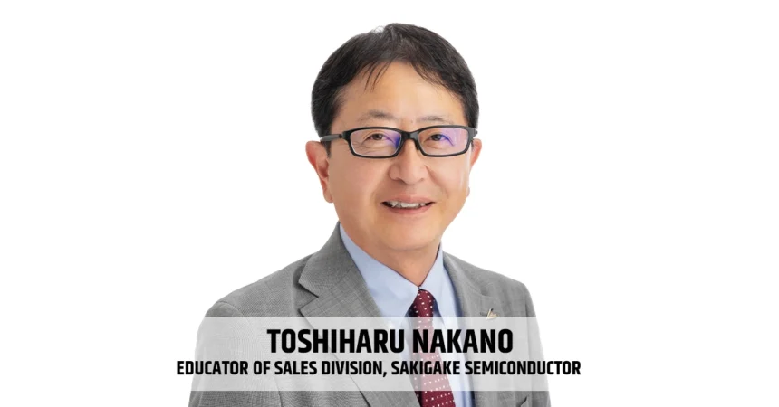
| Toshiharu Nakano – Educator of Sales Division, SAKIGAKE Semiconductor Born on April 25, 1957, in Kanagawa, Japan, Toshiharu Nakano began his career in 1983 at Hosokawa Micron Corporation, a publicly listed company. During his tenure, he held key roles within the Powder Systems Business Division, serving as Kyushu Sales Office Manager and later as Sales Department Manager, overseeing operations across Western Japan, including China, Korea, and Malaysia. In 2014, he joined Sakura Seisakusho Co., Ltd. as Head of the Sales Division. By 2021, he transitioned to SAKIGAKE Semiconductor Co., Ltd., where he currently leads sales efforts. His responsibilities include: • Presenting plasma technology and products to domestic companies, national research institutesand universities, while managing equipment sales, contract processing, and rental services. • Collaborating with distributors to implement effective sales strategies despite limited personnel. • Formulating overseas market strategies by establishing relationships with local sales agents nd partner companies. Nakano plays a pivotal role in strengthening SAKIGAKE Semiconductor’s market position and advancing its asma technology solutions both in Japan and globally. |